
How to analyze Morphology of Polymers using SCANNING ELECTRON MICROSCOPE (SEM)
Principle :
The principle of a scanning electron microscope or SEM functions by scanning a finely focused beam of electrons onto a sample.
The impinging electrons interact with the samples molecular composition.
The energy of the impinging electrons onto a sample is directly in proportion to the type of electron interaction that is generated from the sample.
A series of measurable electron energies can be produced which are analyzed by a sophisticated microprocessor that creates a pseudo three-dimensional image or spectrum of the unique elements that exist in the sample analyzed.
Scanning electron microscopy is used for inspecting topographies of specimens at very high magnifications using a piece of equipment called the scanning electron microscope.
Significance
- SEM magnifications can go to more than 300,000 X.
- SEM inspection is often used in the analysis of cracks and fracture surfaces, bond failures and physical defects on surface.
- SEMs are patterned after Reflecting Light Microscopes and yield similar information:
Topography: The surface features of an object or “how it looks”.
Morphology: The shape, size and arrangement of the particles making up the object that is lying on the surface of the sample or has been exposed by grinding or chemical etching.
Composition: The elements and compounds the sample is composed of and their relative ratios, in areas ~ 1 micrometer in diameter
Crystallographic Information: The arrangement of atoms in the specimen and their degree of order; only useful on single-crystal particles >20 micrometers
Sample Preparation
- Conductive Coating – An ultrathin coating of electrically-conducting material deposited either by high vacuum evaporation or by low vacuum sputter coating of the sample to prevent the accumulation of static electric fields at the specimen due to the electron irradiation required during imaging.
- Such coatings include gold, gold/palladium, platinum, tungsten, graphite etc.
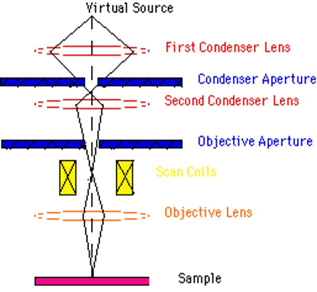
Working Principle

- The “Virtual Source” at the top represents the electron gun, producing a stream of monochromatic electrons.
- The stream is condensed by the first condenser lens (usually controlled by the “coarse probe current knob”). This lens is used to both form the beam and limit the amount of current in the beam. It works in conjunction with the condenser aperture to eliminate the high-angle electrons from the beam
- The beam is then constricted by the condenser aperture (usually not user selectable), eliminating some high-angle electrons
- The second condenser lens forms the electrons into a thin, tight, coherent beam and is usually controlled by the “fine probe current knob”
- A user selectable objective aperture further eliminates high-angle electrons from the beam
- A set of coils then “scan” or “sweep” the beam in a grid fashion (like a television), dwelling on points for a period of time determined by the scan speed (usually in the microsecond range)
- The final lens, the Objective, focuses the scanning beam onto the part of the specimen desired.
- When the beam strikes the sample (and dwells for a few microseconds) interactions occur inside the sample and are detected with various instruments
- Before the beam moves to its next dwell point these instruments count the number of interactions and display a pixel on a CRT whose intensity is determined by this number (the more reactions the brighter the pixel).
- This process is repeated until the grid scan is finished and then repeated, the entire pattern can be scanned 30 times per second.
Test Process:
During SEM inspection, a beam of electrons is bombarded (primary electrons) on a spot of the specimen, resulting in the transfer of energy to the spot.
Primary electrons dislodge from the specimen itself.
The dislodged electrons (secondary electrons) are attracted and collected by a positively biased grid or detector and then translated into a signal.
To produce the SEM image, the electron beam is swept across the area being inspected, producing many such signals.
These signals are then amplified, analyzed and translated into images of the topography being inspected.
Finally, the image is shown on a CRT.
When performing SEM inspection, the following must be observed:
- The EHT must be high enough to provide a good image but low enough to prevent specimen charging.
To maximize contrast due to material differences, use as low an EHT as possible.
- If possible, sputter-coat the specimen to prevent specimen charging. Sputter-coating is considered destructive. Never sputter-coat units that still need to undergo electrical testing, curve tracing, EDX analysis, inspection, etc.
The probe current must be set to its default value, unless a higher probe current is needed to focus the point of interest properly


Post Comment